Page 127 - Combine
P. 127
International Journal of Trend in Scientific Research and Development (IJTSRD) @ www.ijtsrd.com eISSN: 2456-6470

        When  studying  the  APV  effect  in  films  of  elementary   from these materials makes it possible to obtain high-quality
        semiconductors (Si, Ge, and Se) and binary semiconductor   APV films with stable parameters for optoelectronic devices
        compounds,  it  was  found  that  films  made  of  binary   based on the APV effect.
        compounds    have   relatively   positive   degradation
                                                               Physical methods for studying the composition of materials
        characteristics. For example, in CdTe and Sb2Se3 APV films,
                                                               play the most important role in the study of the production
        the aging rate occurs at a low rate.
                                                               technology of APV films.
        Therefore,  the  choice  of  a  suitable  material  and  the
        development of a technology for the production of APV films

                                                         Table 1
                Sample number  Substrate temperature  Evaporation rate, mg / min  Sample resistance, Ohm
                                                                                               5
                      К31                 100                       3                       10
                                                                                               5
                      К51                 150                       3                       10
                                                                                                5
                      К53                 150                      0,5                     5×10
                      К45                 200                       5                       10
                                                                                               5
                      К47                 200                       3                       10
                                                                                               6
                                                                                                6
                      К67                 250                       1                      5×10
                                                                                               6
                      К65                 250                       5                       10
                                                                                               7
                      К72                 300                      0,5                      10
                      К75                 300                       6                       10
                                                                                               6
                      К81                 350                       5                       10
                                                                                               6
                                                                                               7
                      К93                 400                       3                       10
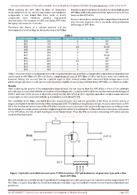
        Table 1 lists some features and parameters of the evaporation process, as well as recommended evaporators for materials that
        can be used in APV films of CdTe and Sb2Se3, comprehensive tests of APV films of CdTe and Sb2Se3 were not carried out,
        however,  taking  into  account  that  for  a  period  equal  to  After  several  weeks,  their  abnormal  high-voltage  open-circuit
        photovoltage and short-circuit current have decreased slightly, it can be assumed that these APV films are relatively stable.
        Results
        After analyzing the graphs of the temperature dependences, we can assume that the APV effect in films of the cadmium
        telluride type is associated with the summation of the voltages of p – n junctions formed at the interface between the hexagonal
        (0001) and cubic (111) phases. It should be noted that the APV effect in CdTe: Ag films and other complex semiconductor
        compounds are also associated with the p-n transition mechanism [9-10].
        The resistivity of the films, calculated from the measured value of ρ and the geometry of the films, is several orders of
        magnitude higher than the resistivity of the starting material. This indicates the presence of high-resistance interlayers in APV
        films. For the Dember mechanism of the APV effect, the role of such interlayers is fundamentally important, since they prevent
        the exchange of current carriers between neighboring photo-active microelements. In films with the p-n transition mechanism
        of the APV effect, the role of such interlayers is not fundamental. Thus, the film is a battery consisting of N active sections
        separated by interlayers.


          Figure 1 Optically controlled microcircuits: T-MOS transistor, FGT-photodetector of generator type with a thin-
                                                      layer APV-film.

        Microelectronics is currently facing the problem of creating microcircuits operating in the nanowatt power range (about 10-9
        W). Thus, it is quite clear that the creation of such microcircuits requires a radical revision of many traditional methods and
        provisions.

        ID: IJTSRD40077 | Special Issue on Innovative Development of Modern Research                     Page 122

